CityU: world’s first university to manufacture next-generation, self-designed compact electron microscopes
A research team at City University of Hong Kong (CityU) is pioneering advanced technology for the next-generation self-design and manufacture of electron microscopes (EMs). CityU is the first university in the world to achieve this.

Credit: City University of Hong Kong
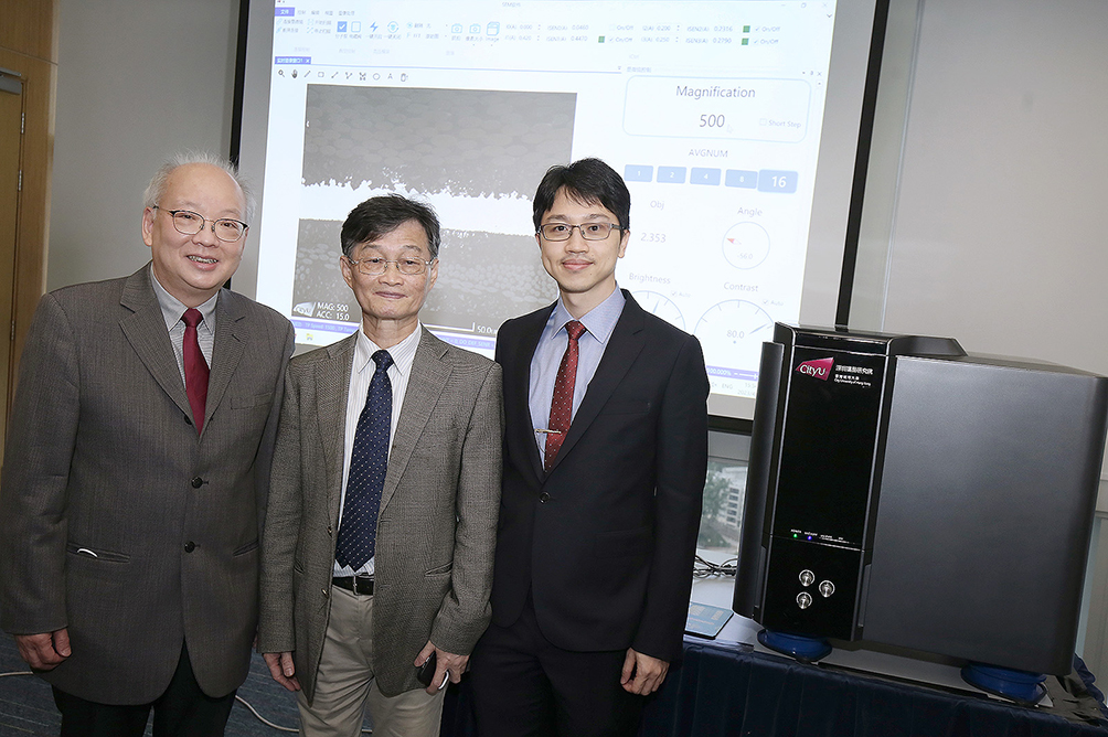
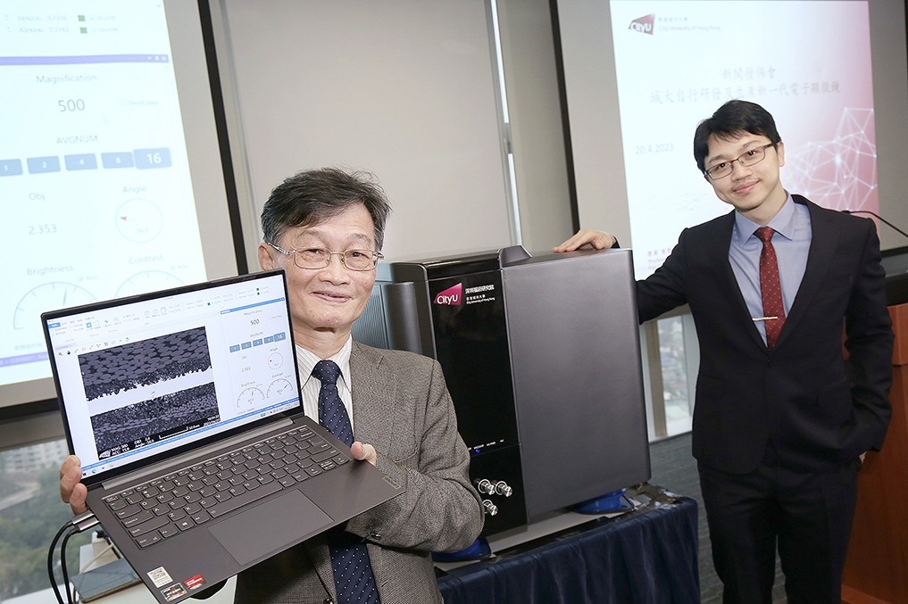
An EM system composed of a pulsed electron source, a fast camera, a staged pumping vacuum system, and an aberration corrector has been developed by a team led by Professor Chen Fu-rong, Chair Professor in the Department of Materials Science and Engineering. It is the first time-resolved electron microscope integrated with both scanning and transmission electron microscope modes in a compact format developed by a university-based research team.
The team’s ultimate goal is to develop a miniature high space-time resolved “quantum” EM that can be used to study atom dynamics of beam-sensitive materials.
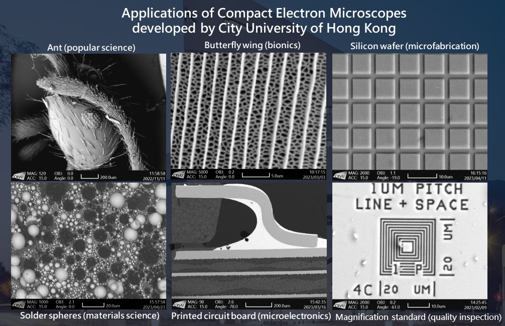
Since EMs are capable of imaging at a significantly higher resolution than light microscopes and provide measurements and analysis at the micro-nano, and even the atomic scale, they are much sought after, especially in medicine, life science, chemistry, materials, integrated circuits and other research industries.
The team has overcome some longstanding problems in the development of EMs. Currently, EMs cannot overcome the scientific bottleneck of radiation damage on a sample and being limited to a static view of the sample, hindering their capability for studying small molecule and electron beam-sensitive materials. Furthermore, their size limits their application in space-expensive environments, such as space shuttles, and deep sea and deep earth research ships and devices.

To overcome these limitations, the CityU research team innovated a differential pumping design to improve the image quality, and developed the backscattered and secondary electron deflectors to enable basic scanning, magnification, imaging functions and observation of liquid samples and beam-sensitive materials.
The team also designed pulsed electron sources and the fast camera that can be used with a desktop EM. By equipping the fast camera with a deflector, the speed of imaging is not limited to the readout time. This is the first time that such a concept can be verified on a desktop EM system. Besides, the team designed an aberration corrector, which can further improve imaging resolution.
With innovative designs mentioned above, the novel EM can generate an image of a sample in five minutes, achieving nanoscale spatial resolution and a magnification of over 105 time for observation and analysis in nanoscale.
In the future, with the ability to independently design and hold intellectual property rights, the team will be able to produce customised miniature EMs at a lower cost. For instance, the LaB6 desktop electron microscope is expected to be sold at 60% of the price of similar products on the market. “The miniaturisation of high-end instruments is an inevitable trend in industrial development,” said Professor Chen, concurrently Director of the Time-Resolved Aberration-Corrected Environmental EM Unit and Director of the Shenzhen Futian Research Institute at CityU.
With the support of the Futian District Government, the team is the only university-based research group to have produced several high-end EMs.
The research team is developing a high spatio-temporal resolution desktop scanning transmission electron microscope (STEM) that utilises pulsed hollow cones to enable observation and reconstruction of protein structures in 3D in room temperature and liquid conditions. This overcomes the current limitation of observing protein structures only under extremely low-temperature conditions using cryo-electron microscopy.
The next stage is to establish a world-leading electro-optical design and manufacturing centre in the Greater Bay Area that will focus on technology transfer and research into electron optics technology.

“This centre aims to spin off electron optics-related technologies for established and start-up companies,” said Professor Chen.
The goal is to stay 15 years ahead of the world’s other EM user facilities in terms of instrumentation and science, he added.
The centre will be organised around novel electron optics for servicing a series of high space/time resolution EMs dedicated to science applications, such as artificial photosynthesis, quantum materials and water science, in environments with a varied range of external stimuli (for example, electric fields, lasers, high temperatures and low temperatures) that are not accessible today.
This platform will lead to breakthroughs in quantum devices, future energy, life science and medicine, said Professor Chen, thereby helping to transform the team’s research findings into applications with real-world benefits, and stimulating collaboration between industry and academia.
Professor Chan Chi-hou, CityU Acting President, Mr Huang Wei, Secretary of the CPC Futian District Committee, Mr Ouyang Huiyu, Vice-District Mayor of the Futian District People’s Government, and Mr Chen Wenhsien, Chief of Science and Technology Major Project Division, Science, Technology and Innovation Commission of Shenzhen Municipality attended the press conference held on 20 April.
