Published on nature nanotechnology (12 December 2022)
Author(s): Wei Han, Xiaodong Zheng, Ke Yang, Chi Shing Tsang, Fangyuan Zheng, Lok Wing Wong, Ka Hei Lai, Tiefeng Yang, Qi Wei, Mingjie Li, Weng Fu Io, Feng Guo, Yuan Cai, Ning Wang, Jianhua Hao, Shu Ping Lau, Chun-Sing Lee, Thuc Hue Ly , Ming Yang & Jiong Zhao
Abstract
Memory transistors based on two-dimensional (2D) ferroelectric semiconductors are intriguing for next-generation in-memory computing. To date, several 2D ferroelectric materials have been unveiled, among which 2D In2Se3 is the most promising, as all the paraelectric (β), ferroelectric (α) and antiferroelectric (β′) phases are found in 2D quintuple layers. However, the large-scale synthesis of 2D In2Se3 films with the desired phase is still absent, and the stability for each phase remains obscure. Here we show the successful growth of centimetre-scale 2D β-In2Se3 film by chemical vapour deposition including distinct centimetre-scale 2D β′-In2Se3 film by an InSe precursor. We also demonstrate that as-grown 2D β′-In2Se3 films on mica substrates can be delaminated or transferred onto flexible or uneven substrates, yielding α-In2Se3 films through a complete phase transition. Thus, a full spectrum of paraelectric, ferroelectric and antiferroelectric 2D films can be readily obtained by means of the correlated polymorphism in 2D In2Se3, enabling 2D memory transistors with high electron mobility, and polarizable β′–α In2Se3 heterophase junctions with improved non-volatile memory performance.
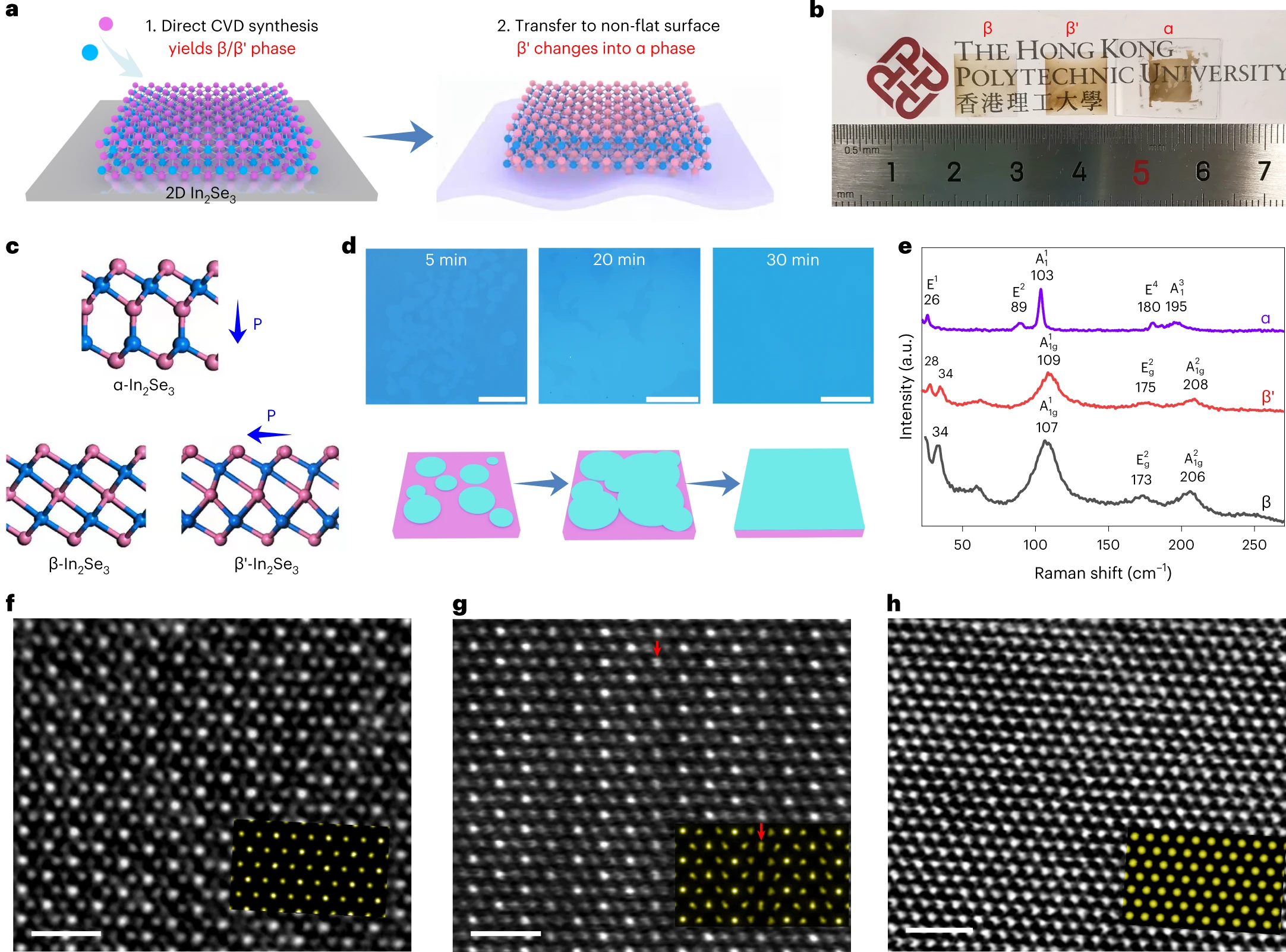
Fig. 1 | Phase-controlled synthesis of large-area 2D In2Se3 films. a, Schematic of the controlled synthesis of β-, β′- and α-In2Se3 films. The β and β′ phases were directly grown by CVD and the α phase was obtained by phase transition after transferring the β′ phase to non-flat surfaces. The pink balls represent the gaseous Se precursor, and the blue balls represent the gaseous In-containing precursor (In2O3–xSex and/or InSe1+y). b, Photograph of the obtained large-area In2Se3 films of three phases (β and β′ on mica and α on PET). c, Side-view crystal models simulated by DFT calculations on α-, β- and β′-In2Se3. The red balls represent Se atoms, and the blue balls represent In atoms. The blue arrows highlight the main polarization directions. d, Growth-time-dependent optical images of β-In2Se3 films at 5, 20 and 30 min (top). Scale bars, 50 μm. Schematic of the growth mechanism of continuous β-In2Se3 films (bottom). It includes three stages: (1) nucleation, (2) growth and merging and (3) stitching. e, Raman spectra of 2D In2Se3 films of the three phases. f–h, Atomic ADF-STEM images of β-In2Se3 (f), β′-In2Se3 (g) and α-In2Se3 (h). The insets show the simulated ADF-STEM images of the corresponding phases. Scale bars, 1 nm.
Read more: https://www.nature.com/articles/s41565-022-01257-3