Opportunity
LEDs are the standard light source used in a wide range of consumer products. However, the current luminescence and cost of LEDs prevent their further commercial use. Manufacturers are investigating patterning sapphire LED substrates to maximize the light emitted while keeping production costs down. Developers have begun to put nanostructures on sapphires by reactive ion etching with a patterned photoresist (PR) mask on top of substrates, which are known as patterned sapphire substrates (PSS). However, creating accurate and uniform high-precision nanostructures on the PR mask with a low-cost and high-throughput process is a challenge in PSS manufacturing. To overcome these issues, researchers have developed a new optimized nano-patterning scheme and demonstrated its use on sapphire substrates. Furthermore, using simulations and modeling the inventors show that the technique is easily scaled to large substrate sizes.
Technology
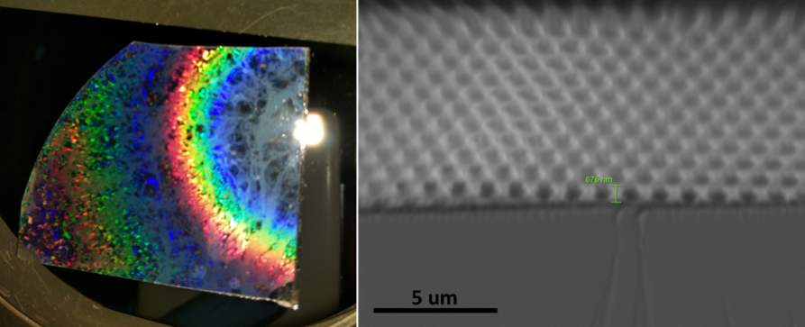
The invention is a low-cost and high-throughput nano-patterning process scheme to achieve accurate and uniform high-precision nanostructures on sapphire substrates to improve LED production. In this novel technique, soft polymer films with controllable surface textures are used with UV flood illumination to construct nanoarrays in the photoresist layer. Various nano-arrays can be achieved on sapphire substrates using conventional etching processes. Two sub-processes are used in the scheme. The first optimizes the different processing conditions, such as soft polymer composition, to achieve a regular and controlled pattern on the polymer mask. The second sub-process optimizes the masking layer for pattern transfer onto sapphire substrates depending on whether dry or wet etching is used.
Advantages
- This polymer-based method can be reused at least 100 times without any distortion of the patterned nano-features
- The technique does not require large pressure and superior substrate flatness for the patterning process
- Expensive or complicated equipment for the patterning is not needed
- The approach is easily scalable to larger substrate sizes
Applications
- The invention is to fabricate enhanced LED devices with the improved luminescence efficiency, which could be applied to general lights, HDTVs, smart phone and computer monitor back lighting.


