Opportunity
Currently, high-gain antennas on the market are either array type which requires complex feeding network or the reflector and lens type which suffers from the inherent drawback of high profile of the whole antenna system.
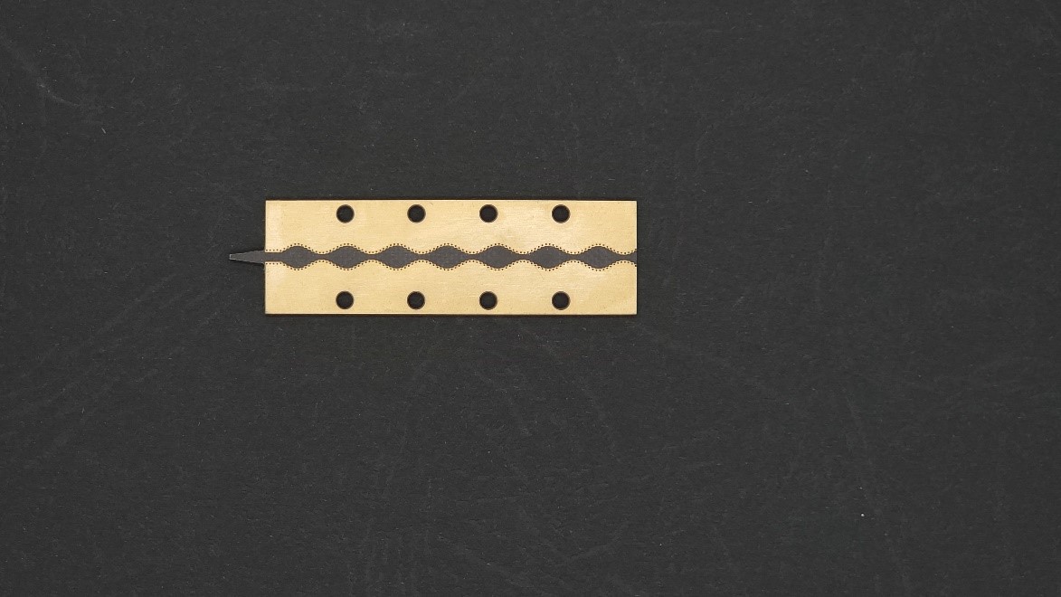
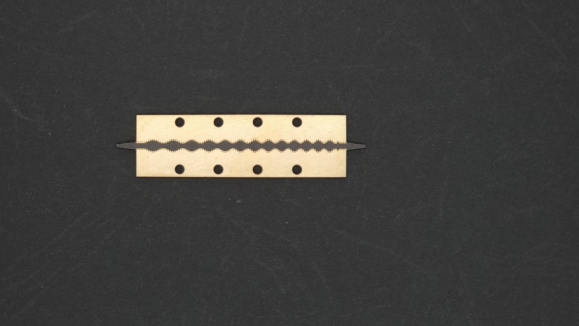
The invention proposes a high-gain antenna application using a novel type of leaky-wave antenna (LWA) by modulating the width (amplitude) of the inset dielectric waveguide. Inset dielectric waveguide, a rectangular groove filled with dielectric, is an effective transmission line because of its low propagation loss and ease of fabrication. By simply varying the width of the inset dielectric waveguide, the wave-guiding structure can work as a high-gain leaky-wave antenna for far-field or near-field focusing applications.
Technology
The novelty of this invention is the modulation of the width of the dielectric waveguide. By implementing different aperture widths along the length of the leaky-wave antenna, the antenna can be used for far field or near field focusing applications.
For far-field high-gain applications, the antenna consists of a taper transition part and a sinusoidal width-modulated substrate integrated inset dielectric waveguide. The whole width-modulated inset dielectric waveguide-based leaky-wave antenna can be implemented in a single-layer PCB substrate. The proposed antenna can also be designed for near-field focusing applications by properly selecting the aperture width variation. The taper transition is identical to that of the far-field case.
Advantages
- Does not require any complex feeding network
- Low profile, simple feeding mechanism and inherent frequency beam scanning capability
- Easily implemented using standard PCB process and integrated with circuits for applications in microwave and millimeter-wave bands
- At terahertz (THz) frequencies, the invention can be implemented using typical CMOS or other similar technologies
Applications
- Applications for millimeter-wave high-gain far-field applications, such as 5G wireless communications and radar systems, as well as for near-field focusing applications such as noncontact sensing, RFID system, millimeter-wave imaging, and wireless transmission energy systems.
- Similar applications can be found in microwave and THz bands, e.g., chip-to-chip or machine-to-machine communications in future 6G.


