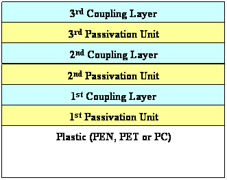
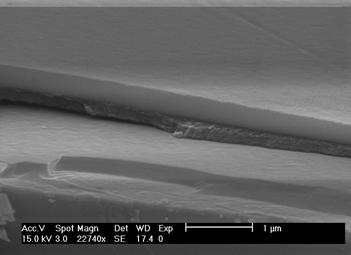
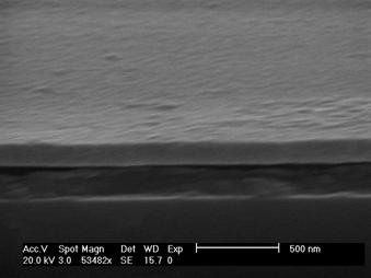
Several problems must be solved before flexible OLEDs can become a reality. The extreme sensitivity of OLEDs to water and oxygen requires an extremely low gas permeability of the substrates that is far from what any known transparent polymeric substrate can achieve. Unlike OLED on rigid glass, the encapsulation for flexible OLED is neither rigid metal sheet or glass caps. An advanced thin film encapsulation technique for FOLED applications is needed. Such an encapsulation scheme demands low gas permeability and "thick" enough to eliminate the dust effect. Besides, the film(s) must prohibit the crack propagation during bending. In fact, exploration of the possible potential of thin films for encapsulation is challenging and 'product-ready' encapsulation has not been achieved yet. Single-layer structure or multilayered structure can be the winner. CityU aims at developing a thin film packaging technique which consists of single layer or multi-layers of nano-scale organic and inorganic thin films, which act as a barrier to protect the electrode and active region from water and oxygen permeation. The films are prepared by magnetron sputtering and chemical vapor deposition. The factors to be noted here are the control of low substrate temperature (< 100oC) and ion bombardment damage so as to minimize damages to the EL organic layer already deposited.
| Plastic | Substrate Thickness (mm) | Passivation Unit | Coupling Layer | No. of Unit | Bending cycles |
|---|---|---|---|---|---|
| PET/PEN | 50 - 75 | - | C1 (150nm) | 1 | 250 |
| PET/PEN | 50 - 75 | P1 (75nm) | C1 (150 nm) | 1 | 1000 |
| PEN | 100 | p1 (75nm) | C1 (150nm) | 1 | 300 |
| PC | 120 - 200 | p1 (75nm) | C1 (150nm) | 1 | 1 - 2 |
| PET/PEN | 50 - 75 | P1 (75nm) | C1 (150nm) | 3 | 250 |
| PET/PEN | 50 - 75 | P1 (25nm) | C1 (50nm) | 3 | 1200 |
| PET/PEN | 50 - 75 | P1 (25nm) | C1 (50nm) | 4 | 800 |
| PET/PEN | 50 - 75 | P1 (75nm) | C2 (150nm) | 1 | 850 |
| PET/PEN | 50 - 75 | p1 (25nm) | C2 (50nm) | 3 | 1000 |
| A Summary of Cyclic Bending Test | |||||