The extreme properties of cBN have prompted material scientists to develop their novel structures and new industrial products. The study on the synthesis and characterization of cBN and diamond started almost together in the early 1960s. To date, cBN has been commercially synthesized in large quantities as powders with sizes ranging from submicron to millimeters by a high-pressure high-temperature (HPHT) method. Abrasive cBN powders are usually cemented by metal binders and formed to fabricate tools of various shapes. Together with HPHT diamond, HPHT cBN has a billion dollars market especially in cutting tools and wear parts. The severe nature of the HPHT methods and the limited size of cBN grains produced, however, prohibit many attractive potential applications of cBN. This is a major motivation for thin film synthesis of both cBN and diamond.
The similarities in structure, properties, technological evolution and application of diamond and cBN suggest that it is worthy to discuss several points related to the synthetic methods of these materials. Diamond films can be prepared in nanocrystalline and polycrystalline forms by using chemical vapor deposition (CVD) methods. CVD diamond films have been already employed in several industrial areas. For example, diamond heat sinks are used in electronic devices. The diamond-coated cutting tools are also commercially available, and they are found to be highly reliable, high-performance and cost-effective tools particularly in machining and cutting hard aluminum alloys. Homoepitaxial diamond single crystals synthesized by CVD are commercially available as well.
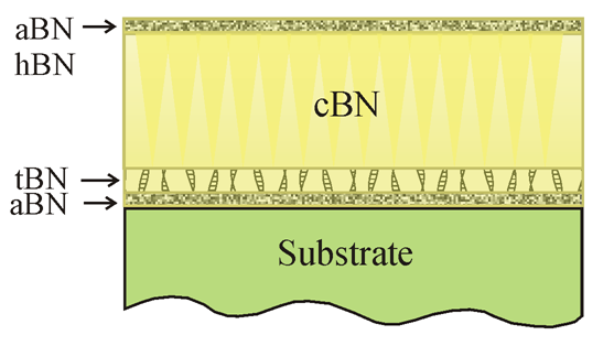
However, although synthesis of cBN by low-pressure methods started historically the same time as diamond synthesis, the cBN film quality lags far behind that of diamond, and cBN films have not been implemented into practice so far. A part of the problems is associated with the deposition techniques themselves. Unlike CVD diamond growth, cBN deposition methods require ion assistance (bombardments) which introduces defects in the films and therefore the structure of cBN films are nanocrystalline, highly defective, and contain other BN phases.
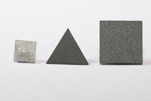 (Left) CVD diamond coating for cutting purpose |
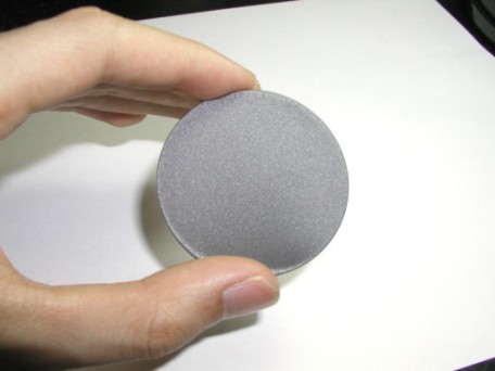 (Right) Thick CVD diamond film (0.2 mm) |
To overcome the illustrated problems, several approaches have been undertaken including: