Several terminologies are used to describe the device characteristics of OLEDs. They include luminance, threshold voltage, efficiency, chromaticity and durability. Luminance is a psychophysical analog of brightness. Threshold voltage is the turn-on voltage for a device to obtain a luminance of 1 cd/m2. Current efficiency is defined as the luminous flux per current passing through the cell. External quantum efficiency is the ratio of number of photons ejected to the number of charges injected into the devices. Chromaticity is a standard way to measure colors of the emitters. Durability is defined as the continuous operation time for a device decaying from its original luminance to its half value. A good OLED should have a low threshold voltage, high quantum efficiency, high current efficiency and long operation lifetime. There are a number of factors that determine the device performance. Threshold voltage is determined by injection barrier (the barrier height at the contacting electrode/organic interface) of the majority carriers. The optimization of device quantum efficiency and current efficiency requires that injection of holes and electrons must be balanced, which are controlled by the matching of their energy levels. The chemistry at the organic/electrode and organic/organic interfaces is a critical factor affecting the operation stability and luminous efficiency. Mismatch of energy level alignments alters the exciton recombination zone and hence modify the emissive color. In other words, efficient charge injection and a balance between the injected electrons and holes are two criteria that must be fulfilled for fabricating an OLED with high efficiency. From the above, we then understand that (i) the barrier heights at the contacting electrode/organic and organic/organic interfaces determine the recombination zone and more critically the device performance such as turn-on voltage and luminous efficiency, and (ii) the chemistry between the electrode and organic materials are also important to the electronic and chemical properties at the interface, which in turns modifies the bulk properties of the OLEDs. From a fundamental point of view, understanding the electronic structures and chemical properties of metal/organic interfaces is of paramount importance in improving the device performance of OLEDs.
We therefore know that the interfaces between metals and organic materials play a crucial role in the OLED performance and therefore electronic properties of their surfaces near the vacuum should be examined. Surface electronic properties of metals and organic materials, such as the work function of metal (fm), work function of organic material (fp), ionization potential (IP), electron affinity (EA) and bandgap (Eg), are determined by the vacuum level (Evac), Fermi Level (Ef), the highest occupied state (HOS) and lowest unoccupied state (LUS). Evac is the energy of an electron at a point sufficiently far away from the surface to be free from the influence of the surface. The work function is defined as the minimum energy required removing an electron from the interior of the solid to a point just outside the solid [1], which corresponds to the energy difference between the Ef and Evac. HOS and LUS are the terminologies to describe the energy levels in an organic semiconductor, which are actually analogous to valence band maximum (VBM) and conduction band minimum (CBM) respectively in inorganic semiconductors. It should be noted that the HOS and LUS are the threshold energy levels for charge injections, while their centroids are called HOMO and LUMO, respectively. IP is the minimum energy required to bring an electron from the HOS in a neutral molecule to the vacuum to form a positive ion, while EA is the minimum energy to form a negative ion. The energy separation from the HOS or LUS to the Evac is then the IP and EA, respectively. fm, fp and IP can be measured by UPS, and EA is typically estimated by the subtraction of bandgap from the IP.
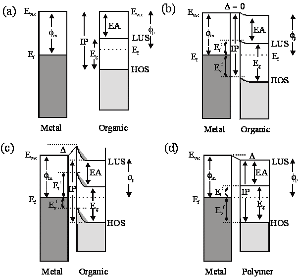
When a metal and an organic material are put together, two regimes define their interface formation. In the early days, it was believed that the energy level alignment at the metal/organic interface, or vice versa, obeyed the Schottky-Mott limit, which is generally used to describe the energy level alignment in inorganic semiconductors. In such a case, the vacuum level between the metal and organic layer is aligned (Figure a). The Schottky-Mott model assumes an ideal and non-interactive metal/organic material interface, without formation of interface electronic states (i.e. no interface dipole). In this metal/organic layer contact, Evac, LUS and HOS are bent by the charge distribution in the semiconductor to achieve electrical equilibrium with the alignment of Ef of these two solids. This process is known as band bending. To use the example in Figure b, the metal layer is more comfortable for an electron as fm is larger than fp, and electrons migrating from the organic layer to the metal side is the consequence, leading to the negative and positive charging of the metal and organic material, respectively. The charging then slows down the movement of electrons to the metal and at the same time redistributes the mobile charge carriers in the organic layer. This flow and redistribution continues till both the Ef between the metal and organic layer are aligned. In this process, the band bending may occur with a depletion region of hundreds of angstroms (Å) in thickness for a semiconductor. This is in contrast to the formation of interface dipole that is constructed abruptly on approximately an order of Å at the metal/organic interface. In the case shown in Figure b, the barrier heights for hole injection Evf and electron injection Efc are simply given by
| (1) | Evf = IP – fm | and | |
| (2) | Efc = fm – EA |
Nevertheless, this rule was broken for most metal/organic interfaces after the first observation of 'vacuum level not aligned' by Narioka et al. using ultraviolet photoemission spectroscopy in 1995. Later, numerous analogous reports in most metal/organic and some organic/organic systems strengthen this scenario. In this system (Figure c), a dipole layer is present at both the organic-on-metal and metal-on-organic interfaces, leading to a steep potential change at these interfaces, and hence the presence of the dipoles creates a discontinuity in the Evac at the interfaces. Using this Ef-aligned approach and the nomenclature reported by Ishii et al. for organic/metal interface, the hole injection Evf and electron injection barriers Efc become
| (3) | Evf = IP – D – fm | and | |
| (4) | Efc = fm – (EA – D) or Eg – Evf |
where D is the interface dipole. Bardeen attributed this discrepancy to the presence of interface states occurring within the bandgap (therefore also referred to as gap states), and Ef is then pinned at the interfaces by these states. It should be noted that the sign of D depends on the direction of the dipole moment. In the case as shown in Figure c, D is positive. In this case, the Evf and Efc cannot be predicted from the simple relationships among fm, IP and EA. Neglecting the significance of D in organic semiconductor may generate an error in predicting the injection barriers of charge carriers, though nowadays the Evac is still always considered as a common reference level, which is a hypothetical concept to make the interpretation simple.
The 'vacuum level not aligned' approach is a better concept to describe the interface electronic states, though, as a matter of fact, no vacuum level exists at the underlying layer. The interface states may originate from intrinsic defects and impurities in the solid, interfacial chemical reaction, charge transfer process across the interface, metal-induced defects, etc. In fact, we can hardly comprehensively manifest an actual polymer/metal interface accurately, in contrast to the ideal organic/metal contact in Figure c, since preparation of polymer films with a thickness of the order of Å by a spin-coating technique is not an easy task. In polymer/metal interfaces, the interfacial dipole D is therefore generally represented as:
| (5) | D = fm – fp |
These relationships are shown in Figure d. The binding energy separation between the HOS and fp of the polymer then represents the barrier height Evf for hole injection, giving
| (6) | IP = fp + Evf | and | |
| (7) | Efc = Eg – Evf |
Using the above definitions, the D on the polymer/metal interface was always found to be null, in contradiction to that on most of the organic/metal interface. The non-zero interfacial dipoles are often observed in the latter case because the vapor deposited molecular species may possess a higher arrival kinetic energy to interact with the metal substrate, resulting in charge transfer or interfacial chemical interactions between the metal and organic material. On the contrary, the presence of solvent from the spin-coated polymer was believed to passivate the above chemistry.
To distinguish between the Schottky-Mott and Bardeen models, it is necessary to prepare organic films and apply them on different kinds of metal substrates. Base on
| (8) | S = dEfc / dfm | and | |
| (9) | S = – dEvf / dfm |
S is unity if the change of Efc or Evf is exactly the difference of fm between two metals, i.e. the Schottky-Mott model. It is also unity when D is independent of the metals. On the contrary, the Bardeen model holds for S < 1.
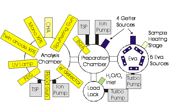
CityU equips with a state-of-the-art surface analytical system (VG ESCALAB 220i-XL) which is able to conduct x-ray photoelectron spectroscopy (XPS), ultra-violet photoelectron spectroscopy (UPS), Auger electron spectroscopy (AES), Auger and x-ray imaging, and scanning electron microscope (SEM). We are interested in looking into the following tasks:
Recent findings: