Facilities and Laboratories

HKICE is a research center that leverages the University's research prowess and resources to achieve breakthroughs in the clean energy field. The integration of cutting-edge laboratories within HKICE facilitates synergies that drive innovation in this field.

Some of the most advanced facilities in the field are the TRACE, the Multifunctional Optical Spectroscopy, and the Integrated Lab Facility for Organic and Organic/Inorganic Hybrid Optoelectronic Devices. The first two facilities boast unique, custom-built systems that push the limits of both spatial and time resolution, allowing for in-situ studies on charge dynamics at the atomic level; while the integrated lab facility provides researchers with a platform for interdisciplinary for different organic optoelectronic devices.


Together, these cutting-edge facilities have far-reaching implications in different areas, such as aerospace and medicine. The remarkable capabilities of these labs and the exciting advancements they are making in materials science and engineering are an important track record of their significance.

HKICE is at the forefront of clean energy research, driving innovation and contributing to the advancement of science and technology. 

State-of-the-Art 
Facilities in HKICE

Time-resolved Aberration Corrected Environmental (TRACE) EM Unit 

The Multifunctional Optical Spectroscopy and Imaging System

Integrated Lab Facility for Organic and Organic/Inorganic Hybrid Optoelectronic Devices 

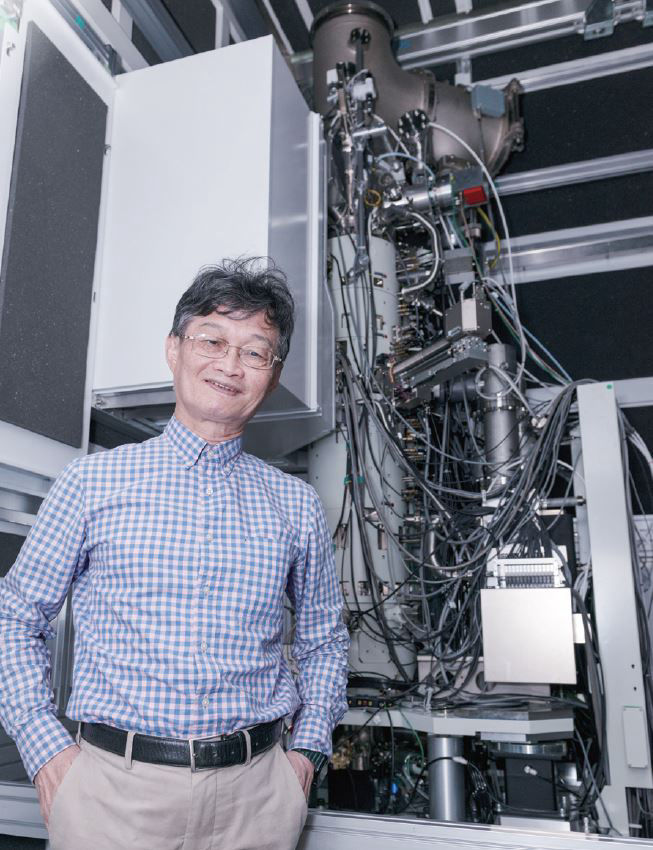
Time-resolved Aberration Corrected Environmental (TRACE) Electron Microscope

Facilities In-charge: Fu-Rong CHEN

TRACE is a unique facility in CityU that could allow cutting-edge analysis at the atomic scale. This powerful microscope uses pioneering technology that allows Prof. CHEN and his researchers to be the first group of scientists to observe material properties at an atomic level – actually seeing the atoms moving very fast in 3D instead of 2D static images.

The cutting-edge technology in this microscope is twofold. Not only can it display atoms moving in 3D, but also allow the recovery of 2D images into 3D dynamics. 
TRACE is equipped with an ultrafast pulsed electron source that could offer a much softer touch to the testing materials. It thus helps to maintain the integrity of the samples during the investigation. At the same time, the atomic-resolution structure and dynamics can be recorded with synchronization of ultrafast electron and fast-speed single electron sensitive camera. By gaining a better understanding of the structure of the materials under study, we can understand their physical properties to better develop new materials.

“All technology stems from new material innovation and this microscope can help us make better materials for clean energy,” says Prof. Chen. “Special instrumentation is needed for innovations and here at CityU our microscope
is unique.”

Usually, the atomic resolution of materials can be revealed for crystalline materials along a few particular crystallographic orientations, breakthroughs have already been made in resolving in 3D atom dynamics at spacetime resolution of 10-10 m.sec for helix materials including carbon nanotubes and single double-strand DNA from the TRACE TEM in CityU. The highest space-time resolution of 3D atom dynamics can be achieved is 10-13 m.sec in a 2D material, graphene.

Apart from clean energy, numerous industries will benefit from new materials, including IC chips, aerospace, medicine, and daily necessities. For instance, new
alloys with increased strength and toughness that can withstand extreme temperatures can be applied to the aerospace industry.

Read more:

CityU becomes the world’s first university to manufacture next-generation self-designed electron microscopes 
20.04.2023

Multifunctional Optical Spectroscopy and
Imaging System

Facilities In-charge: Dangyuan LEI

This facility contains equipment such as femtosecond laser pump-probe ultrafast spectroscopy, single-particle dark-field scattering imaging and spectroscopy, low-temperature time-resolved photoluminescence spectroscopy, single-photon autocorrelation-function measurement system, and scattering-type scanning near-field optical microscope. This sophisticated equipment can overcome the spatial resolution limit of conventional optical microscopes (i.e. Abbe’s diffraction limit) with a ground-breaking apertureless near-field microscope that combines Atomic Force Microscopy (AFM) with optical imaging and ultrafast spectroscopy at the nanoscale.

It can perform (1) optical near-field mapping and spectroscopy throughout the visible to infrared spectral range all at the spatial resolution down to 10 nm and (2) ultrafast pump-probe spectroscopy at the same spatial resolution, providing unprecedented characterization capabilities for studies of functional nanomaterials, plasmonics, and nanophotonics, biosensing, and bioimaging.


“Most of the measurement systems in our lab are home-built,” Dr. LEI explains. “We designed the whole system by ourselves and assembled them together for multiple functionalities yet at the lowest cost possible.”

Its capabilities include giving measurements in extreme spatial resolution and extreme temporal resolution. This facility can perform nanoscale optical imaging and ultrafast spectroscopic measurements of materials simultaneously.
Prof. LEI sums up its features in two words: “small and fast”.

“Not only can we measure optical properties of tiny objects down to 10 nanometres (nm), but also the ultra-fast dynamics of the materials at a time scale as fast as several tens of femtoseconds (fs),” he says.

In the case of perovskite solar cells, we are striving to enhance their power conversion efficiencies. They need to understand the optical properties of the nanoscaled material and the ultrafast dynamics of their new materials under sunlight illumination, and this facility can fulfill such specific needs.

Integrated Lab Facility for Organic and Organic/Inorganic Hybrid Optoelectronic Devices 

Facilities In-charge: Alex JEN, Angus YIP, Zonglong ZHU

It provides a perfect platform for interdisciplinary research from the most fundamental sciences to realistic applications in daily life.

The facility includes a variety of well-equipped labs for chemical synthesis, material characterization, and thin-film processing, as well as fabrication and testing of devices such as LEDs, solar cells, transistors, photodetectors, etc., and a scale-up lab for large-area processing of thin-film devices.

The culture here encourages researchers with different expertise to work closely together to speed up the feedback loop, therefore pushing forward the vibrant development of organic and organic/inorganic hybrid perovskite materials to fulfill the critical need for clean energy sources of human society.

Follow Us